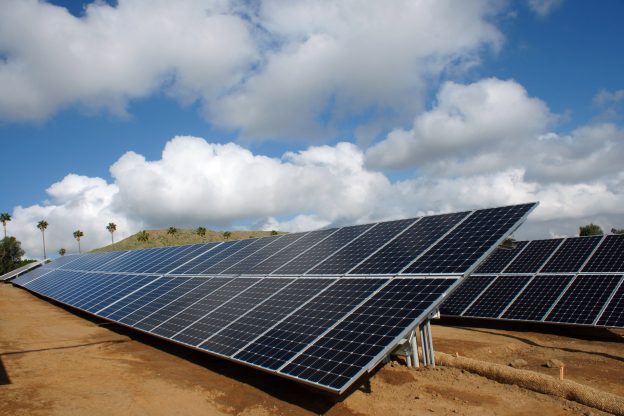
Commercially available solar panels now routinely convert 20% of the energy contained in sunlight into electricity, a truly remarkable feat of science and engineering, considering that it is theoretically impossible for silicon-based solar cells to be more than 32% efficient. This upper bound, known as the Shockley-Queisser Limit, was first calculated by the eponymous scientists (who actually gave 30% as their original limit) in the Journal of Applied Physics in 1961 [1] (see also updates by Rühle [2]).

Now, if we can answer why solar panels are thus limited, we can understand the essentials of photovoltaics (PV), which have their basis in the photoelectric effect, and p-n semiconductor junctions. While many have never heard of it, the photoelectric effect is of monumental importance, and when Albert Einstein received the 1921 Nobel Prize in physics, it was “for his services to Theoretical Physics, and especially for his discovery of the law of the photoelectric effect,” while p-n junctions lie at the foundations of modern electronics, including transistors and LEDs. Indeed, a solar cell is essentially an LED in reverse: Instead of an electric current generating light, light generates electric current!
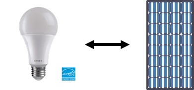
LEDs and solar cells are just the inverses of each other!
The goal of the remainder of this post is to introduce the very basic physics of solar cells, so that as a reader you come away with a basic understanding of the function and limits to solar PV technology. To start, let us outline how crystalline silicon (the basis for virtually all solar cells) can be formed into a p-n junction that generates a useful current, but for this, gentle reader, we must recall some basic chemistry, and turn to our oft-memorized but seldom understood periodic table of elements (and zoom in to the top three rows), with carbon(C) and silicon (Si) highlighted:
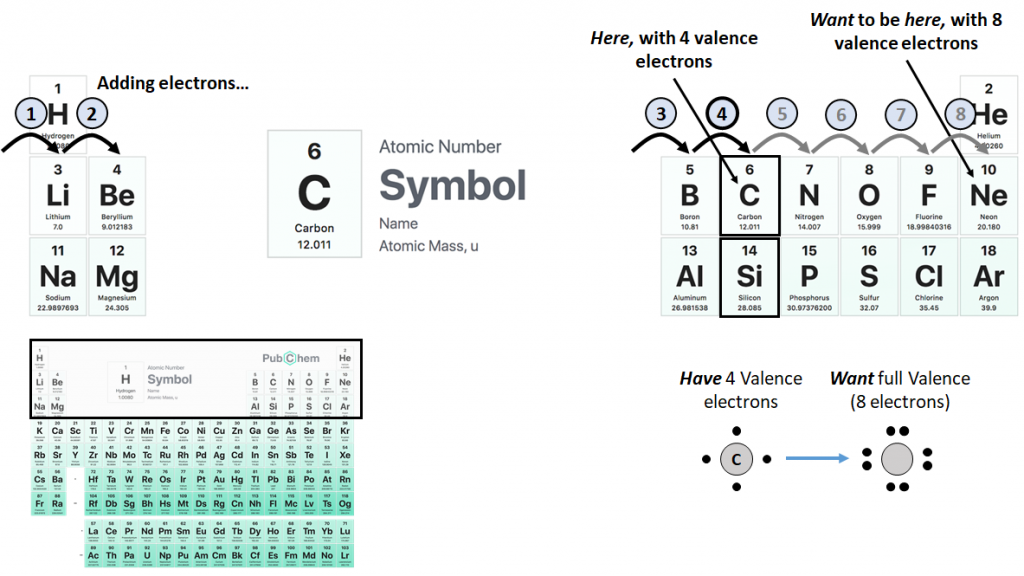
eriodic table of elements and the first few rows highlighted: As we move across columns from left to right, we add electrons to the element’s outermost shell, until a stable, full valence is reached on the right. By virtue of their position in a common column, carbon and silicon have similar chemistries. Periodic table adapted from https://pubchem.ncbi.nlm.nih.gov/periodic-table/ (US government); overall figure by the author. All remaining figures by the author.
Now, all the elements on the rightmost column are happy and fulfilled, and are known as the noble gases, for such is their majesty that they do not deign to react with the other peasant elements. And of course, all other elements wish to be as these haughty few. Why is this?
It is because electrons surrounding an atomic nucleus are restricted to certain orbitals which can contain only a fixed number of electrons, proceeding outward from the nucleus in “shells,” with electrons added and removed only from the outermost, or “valence,” shell. The periodic table summarizes the state of the valence shell: In essence, as we start on the leftmost column and go to the right, we add electrons to the valence shell. Carbon and silicon have four valence electrons, but if we could add another four, making eight and a “full valence,” we would become as the noble gases on the right.
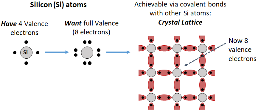
How to do this? Share electrons with another atom, and be thus bonded together (forming a “covalent” bond)! Carbon is especially promiscuous in this, and the vast array of molecular configurations that may use carbon as a backbone make up the basis of all life on Earth (silicon has a lesser, but similar, character, hence the sci-fi trope of silicon-based life). Noble gases have no need to share electrons, hence their imperious ways.
One way to give a collection of silicon atoms full valences is to form a (tetrahedral) crystal lattice, where each atom shares one of its electrons with another atom, like so:
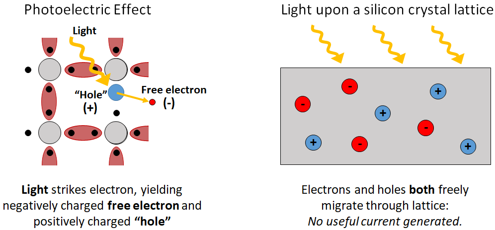
Now that we have a crystal silicon lattice, let’s introduce the photoelectric effect, wherein sunlight falling upon this lattice may strike an electron, knocking it out of its covalent bond (the electron is then said to enter the conduction band), allowing it to migrate freely (and randomly) through the lattice. When such a negatively charged “free electron” begins wondering, it necessarily leaves behind an unpaired electron and a positively charged “hole.” Like the free electron, as electrons un-pair and re-pair, the hole can also migrate randomly through the lattice. In a pure Si lattice, light and the attendant photoelectric effect does nothing more than create electron-hole pairs that diffuse randomly until recombining, generating no useful current (remember that current is the ordered flow of charge):
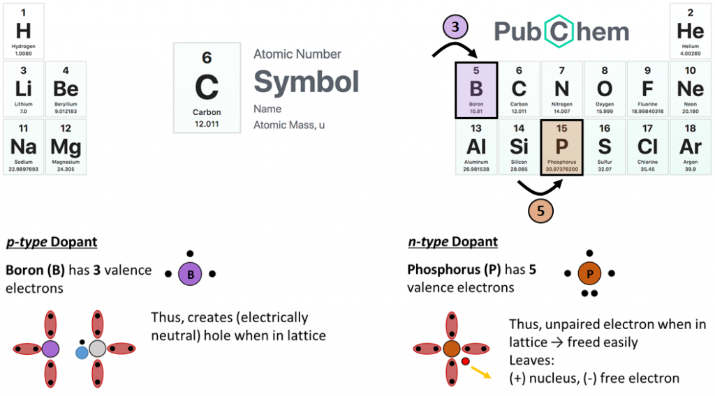
So, to actually utilize the photoelectric effect, we must force excited electrons to flow in a preferential direction (and hence generate current), a task accomplished through the addition of impurities, or “dopants,” into our crystal lattice. There are two basic dopant types:
- n-type (e.g. phosphorus), which adds un-paired electrons to the lattice, and
- p-type (e.g. boron), which creates holes in the lattice.
With a quick look at our periodic table, we can see how phosphorus and boron impurities add unpaired electrons and holes to a silicon lattice:
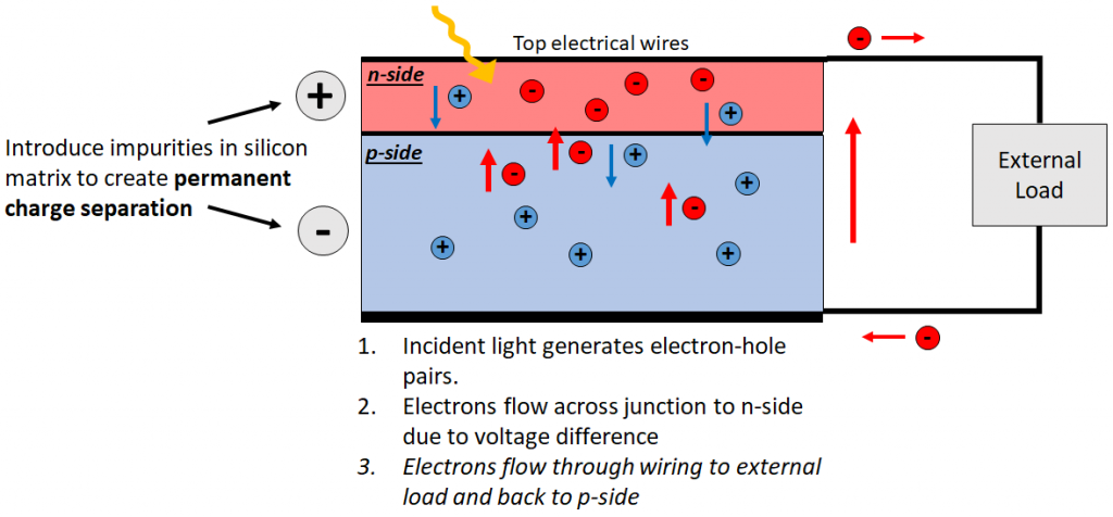
If we stack n-doped silicon on p-doped silicon, un-paired electrons from the n-side fill holes on the p-side, and thus the n-side develops a permanent net positive charge (as it has lost electrons), while the p-side becomes permanently negative. With this charge separation, we can create a useful current loop: When we shine a light on the p-n junction, excited electrons flow unidirectionally to the positively charged n-type silicon. We then place wires on the silicon surface to collect up electrons, connect to an external load, and back to the p-type silicon, and thus electrons are driven in a closed loop, generating electrical current. Voila! A solar cell is born!
Finally, we reach the crux of the matter: Why can a silicon solar cell so constructed never convert more than 32% of incident light into useful current? For p-n solar cells, light energy is lost via three fundamental mechanisms:
- Spectrum losses: At most about 50% of light energy yields photoexcitation, as explained below.
- Radiative recombination: Some electrons randomly fill holes before they can generate a useful current, and about 25% of light energy is lost to this.
- Current impedance: About 14% of energy is lost via resistance to current flow.
Spectrum losses are the dominant factor, and the most interesting, and arise because longwave (e.g., far infrared) light lacks the energy to excite electrons, while shortwave (e.g., ultraviolet) light has an excess of energy. That is, to excite a valence electron to the conduction band requires a specific amount of energy, no more and no less, known as the band gap energy, E, which is about 1.1 “electron-volts” (eV) for silicon (one eV is an almost unimaginably small amount of energy, but appropriate when dealing with single subatomic particles). Light has a dual wave and particle nature, with individual photons (the “particles” of light) having a fixed amount of energy determined solely by the wavelength of light, where the shorter the wavelength, the more energy.
Photons of energy less than 1.1 eV are unable to induce photoexcitation, and thus longwave infrared solar radiation is useless to a solar cell. Further, since it requires 1.1 eV, and only 1.1 eV, to generate an electron-hole pair, any photon energy above the band gap is wasted as heat. Given the spectrum of light hitting the Earth’s surface (at solar noon), we can determine that only about 50% of the Sun’s incoming energy can be converted into electron-hole pairs, beginning with the following schematics illustrating this notion:

The left-hand figure gives the solar spectrum in terms of wavelengths hitting the surface of the Earth (as well as the “top of the atmosphere”). On the right side, the energy of a photon with any given wavelength is indicated by the blue curve: Any electron with a wavelength above about 1,150 nm carries less than 1.1 eV, and so its energy is lost. For electrons with shorter wavelengths, only 1.1 eV is used for photoexcitation, and so the energy gap between 1.1 eV and whatever the photon carries is wasted. The inscribed spectrum is simply for reference (not to scale).
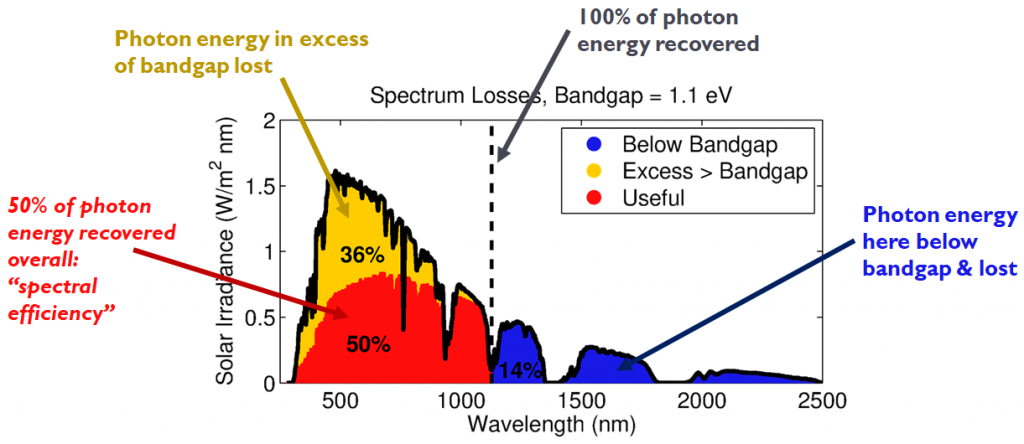
Energy losses and “spectral efficiency” based on a standard solar spectrum and a band gap energy of 1.1 eV.
To see what band gap best balances the two forms of energy loss, we systematically change the band gap energy and make another version of the above figure, tabulating the results (obviously we make a computer do the details!), for example:
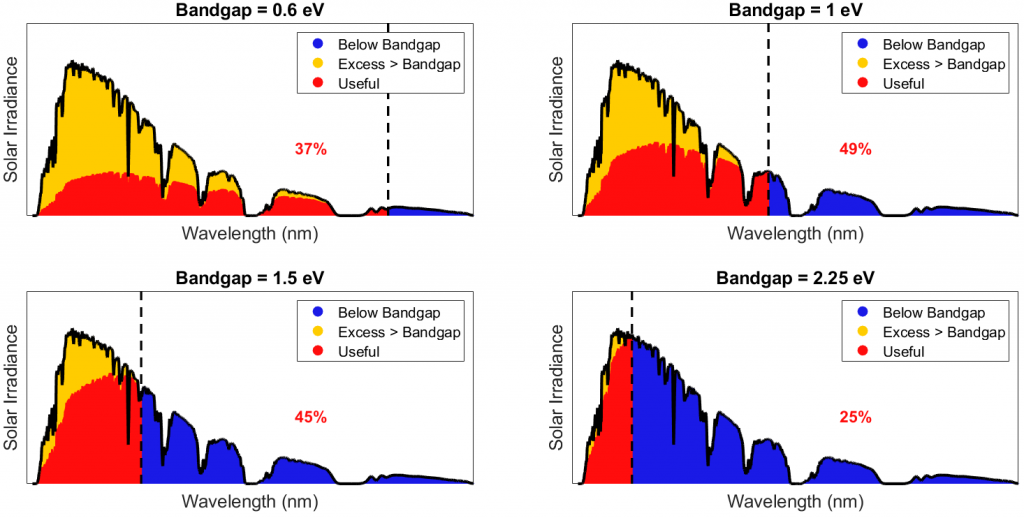
Thus, spectral efficiency indeed peaks at very nearly the 1.1 eV band gap of silicon. Finally, by adding in our energy losses from radiative recombination and circuit resistance, we can determine theoretical maximum efficiency as a function of a solar cell’s material band gap:

Thus, silicon, at about 32% theoretical maximum efficiency, is very nearly the optimum possible material for any solar cell. This limit applies only to single p-n junction cells, and novel PV technologies that involve stacking multiple p-n junctions, for example, can exceed the Shockley-Quiesser Limit. However, as I’ll demonstrate further in another post, the routine 15–20% efficiencies achieved by existing commercial panels are more than sufficient to power global society on a remarkably small slice of land, and there is certainly no need to hold out for greater efficiencies if one is contemplating solar themselves. So finally, let us end with a few summary points:
Key Points
- Solar cells are based on p-n semiconductor junctions and the photoelectric effect
- Sunlight creates “electron-hole pairs” in a silicon matrix via the photoelectric effect
- Dopants in this matrix create a permanent charge separation in the matrix
- This allows free electrons generated by photoelectric effect to flow across an external load and generate useful current
- Band-gap = photon energy required to create electron-hole pair (measured in eV). If an incoming photon has…
Less energy = no effect
Any excess energy = wasted - 1.1 eV for silicon is close to optimum for the Sun’s light spectrum
- Spectral losses + radiative recombination + circuit resistance limit theoretical PV efficiencies
- Silicon PV is limited to 32% efficiency
- Typical commercial tech (15–20%) is already amazing
References
[1] Shockley, W., & Queisser, H. J. (1961). Detailed balance limit of efficiency of p‐n junction solar cells. Journal of applied physics, 32(3), 510–519.
[2] Rühle, S. (2016). Tabulated values of the Shockley–Queisser limit for single junction solar cells. Solar Energy, 130, 139–147.
See also the medium.com version
